William Shockley
William Shockley was born in London on February 13th, 1910 and is the Physicist. At the age of 79, William Shockley biography, profession, age, height, weight, eye color, hair color, build, measurements, education, career, dating/affair, family, news updates, and networth are available.
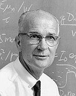

At 79 years old, William Shockley physical status not available right now. We will update William Shockley's height, weight, eye color, hair color, build, and measurements.
Shockley was one of the first recruits to Bell Labs by Mervin Kelly, who became director of research at the company in 1936 and focused on hiring solid-state physicists. Shockley joined a group headed by Clinton Davisson in Murray Hill, New Jersey. Executives at Bell Labs had theorized that semiconductors may offer solid-state alternatives to the vacuum tubes used throughout Bell's nationwide telephone system. Shockley conceived a number of designs based on copper-oxide semiconductor materials, and with Walter Brattain unsuccessfully attempted to create a prototype in 1939.
Shockley published a number of fundamental papers on solid state physics in Physical Review. In 1938, he received his first patent, "Electron Discharge Device", on electron multipliers.
When World War II broke out, Shockley's prior research was interrupted and he became involved in radar research in Manhattan (New York City). In May 1942, he took leave from Bell Labs to become a research director at Columbia University's Anti-Submarine Warfare Operations Group. This involved devising methods for countering the tactics of submarines with improved convoying techniques, optimizing depth charge patterns, and so on. Shockley traveled frequently to the Pentagon and Washington to meet high-ranking officers and government officials.
In 1944, he organized a training program for B-29 bomber pilots to use new radar bomb sights. In late 1944 he took a three-month tour to bases around the world to assess the results. For this project, Secretary of War Robert Patterson awarded Shockley the Medal for Merit on October 17, 1946.
In July 1945, the War Department asked Shockley to prepare a report on the question of probable casualties from an invasion of the Japanese mainland. Shockley concluded:
This report influenced the decision of the United States to drop atomic bombs on Hiroshima and Nagasaki, which preceded the surrender of Japan.
Shockley was the first physicist to propose a log-normal distribution to model the creation process for scientific research papers.
Shortly after the war ended in 1945, Bell Labs formed a solid-state physics group, led by Shockley and chemist Stanley Morgan, which included John Bardeen, Walter Brattain, physicist Gerald Pearson, chemist Robert Gibney, electronics expert Hilbert Moore, and several technicians. Their assignment was to seek a solid-state alternative to fragile glass vacuum tube amplifiers. Its first attempts were based on Shockley's ideas about using an external electrical field on a semiconductor to affect its conductivity. These experiments failed every time in all sorts of configurations and materials. The group was at a standstill until Bardeen suggested a theory that invoked surface states that prevented the field from penetrating the semiconductor. The group changed its focus to study these surface states and they met almost daily to discuss the work. The rapport of the group was excellent, and ideas were freely exchanged.
By the winter of 1946 they had enough results that Bardeen submitted a paper on the surface states to Physical Review. Brattain started experiments to study the surface states through observations made while shining a bright light on the semiconductor's surface. This led to several more papers (one of them co-authored with Shockley), which estimated the density of the surface states to be more than enough to account for their failed experiments. The pace of the work picked up significantly when they started to surround point contacts between the semiconductor and the conducting wires with electrolytes. Moore built a circuit that allowed them to vary the frequency of the input signal easily. Finally they began to get some evidence of power amplification when Pearson, acting on a suggestion by Shockley, put a voltage on a droplet of glycol borate placed across a P–n junction.
Bell Labs' attorneys soon discovered Shockley's field effect principle had been anticipated and devices based on it patented in 1930 by Julius Lilienfeld, who filed his MESFET-like patent in Canada on October 22, 1925. Although the patent appeared "breakable" (it could not work) the patent attorneys based one of its four patent applications only on the Bardeen-Brattain point contact design. Three others (submitted first) covered the electrolyte-based transistors with Bardeen, Gibney and Brattain as the inventors.
Shockley's name was not on any of these patent applications. This angered Shockley, who thought his name should also be on the patents because the work was based on his field effect idea. He even made efforts to have the patent written only in his name, and told Bardeen and Brattain of his intentions.
Shockley, angered by not being included on the patent applications, secretly continued his own work to build a different sort of transistor based on junctions instead of point contacts; he expected this kind of design would be more likely to be commercially viable. The point contact transistor, he believed, would prove to be fragile and difficult to manufacture. Shockley was also dissatisfied with certain parts of the explanation for how the point contact transistor worked and conceived of the possibility of minority carrier injection.
On February 13, 1948, another team member, John N. Shive, built a point contact transistor with bronze contacts on the front and back of thin wedge of germanium, proving that holes could diffuse through bulk germanium and not just along the surface as previously thought.: 153 : 145 Shive's invention sparked Shockley's invention of the junction transistor.: 143 A few months later he invented an entirely new, considerably more robust, type of transistor with a layer or 'sandwich' structure. This structure went on to be used for the vast majority of all transistors into the 1960s, and evolved into the bipolar junction transistor. Shockley later described the workings of the team as a "mixture of cooperation and competition". He also said that he kept some of his own work secret until his "hand was forced" by Shive's 1948 advance. Shockley worked out a rather complete description of what he called the "sandwich" transistor, and a first proof of principle was obtained on April 7, 1949.
Meanwhile, Shockley worked on his magnum opus, Electrons and Holes in Semiconductors which was published as a 558-page treatise in 1950. The tome included Shockley's critical ideas of drift and diffusion and the differential equations that govern the flow of electrons in solid state crystals. Shockley's diode equation is also described. This seminal work became the reference text for other scientists working to develop and improve new variants of the transistor and other devices based on semiconductors.
This resulted in his invention of the bipolar "junction transistor", which was announced at a press conference on July 4, 1951.
In 1951, he was elected to the National Academy of Sciences (NAS). He was forty-one years old; this was rather young for such an election. Two years later, he was chosen as the recipient of the prestigious Comstock Prize for Physics by the NAS, and was the recipient of many other awards and honors.
The ensuing publicity generated by the "invention of the transistor" often thrust Shockley to the fore, much to the chagrin of Bardeen and Brattain. Bell Labs management, however, consistently presented all three inventors as a team. Though Shockley would correct the record where reporters gave him sole credit for the invention, he eventually infuriated and alienated Bardeen and Brattain, and he essentially blocked the two from working on the junction transistor. Bardeen began pursuing a theory for superconductivity and left Bell Labs in 1951. Brattain refused to work with Shockley further and was assigned to another group. Neither Bardeen nor Brattain had much to do with the development of the transistor beyond the first year after its invention.
Shockley left Bell Labs around 1953 and took a job at Caltech.
Shockley, Bardeen and Brattain received the Nobel Prize in Physics in 1956.
In 1956, Shockley started Shockley Semiconductor Laboratory in Mountain View, California, which was close to his elderly mother in Palo Alto, California. The company, a division of Beckman Instruments, Inc., was the first establishment working on silicon semiconductor devices in what came to be known as Silicon Valley.
Shockley recruited brilliant employees to his company, but alienated them by undermining them relentlessly. "He may have been the worst manager in the history of electronics", according to his biographer Joel Shurkin. Shockley was autocratic, domineering, erratic, hard-to-please, and increasingly paranoid. In one well-known incident, he demanded lie detector tests to find the "culprit" after a company secretary suffered a minor cut. In late 1957, eight of Shockley's best researchers, who would come to be known as the "traitorous eight", resigned after Shockley decided not to continue research into silicon-based semiconductors. They went on to form Fairchild Semiconductor, a loss from which Shockley Semiconductor never recovered and which led to its purchase by another company three years later. Over the course of the next 20 years, more than 65 new enterprises would end up having employee connections back to Fairchild.
A group of about thirty colleagues have met on and off since 1956 to reminisce about their time with Shockley as, the group's organizer said in 2002, "the man who brought silicon to Silicon Valley".